Photonics Essentials: Chapter 4 Problems
Source
Thomas P. Pearsall, Photonics Essentials: An Introduction with Experiments
(McGraw-Hill, 2003), Chapter 4, Electrical Response Time of Diodes,
Problems 4.1–4.4, printed pages 75–76.
Worked solutions
Problem 4.1: A 4 MHz fiber receiver
Brief solution
1. Method.
Silicon loses band-to-band response near \(1.1\ \mu\mathrm m\), whereas germanium still absorbs at \(1.3\ \mu\mathrm m\). Of the two choices,
2. Key step.
3. Answer.
The printed C-V graph shows approximately \(3.5\ \mathrm{nF}\) at zero bias, \(2.0\ \mathrm{nF}\) at \(-2\ \mathrm V\), and \(1.55\ \mathrm{nF}\) at \(-3\ \mathrm V\). Therefore choose at least about \(3\ \mathrm V\) reverse bias, preferably with margin for cable and amplifier input capacitance:
Show detailed steps
Silicon loses band-to-band response near \(1.1\ \mu\mathrm m\), whereas germanium still absorbs at \(1.3\ \mu\mathrm m\). Of the two choices,
The specified relation gives the largest permissible time constant:
With a \(50\ \Omega\) load,
The printed C-V graph shows approximately \(3.5\ \mathrm{nF}\) at zero bias, \(2.0\ \mathrm{nF}\) at \(-2\ \mathrm V\), and \(1.55\ \mathrm{nF}\) at \(-3\ \mathrm V\). Therefore choose at least about \(3\ \mathrm V\) reverse bias, preferably with margin for cable and amplifier input capacitance:
For example, \(-4\ \mathrm V\) gives roughly \(C_D=1.35\ \mathrm{nF}\) and leaves about \(0.24\ \mathrm{nF}\) for parasitics.
Problem 4.2: Junction capacitance
Brief solution
1. Method.
For a one-sided abrupt silicon junction under reverse-bias magnitude \(V_R\),
2. Key step.
3. Answer.
Thus every curve has slope \(1/2\); reverse bias shifts a curve downward by widening the depletion region.
Show detailed steps
For a one-sided abrupt silicon junction under reverse-bias magnitude \(V_R\),
Use \(\epsilon_s=11.8\epsilon_0\), \(\epsilon_0=8.854\times10^{-14}\ \mathrm{F/cm}\), and the representative silicon value \(V_{\mathrm{bi}}=0.8\ \mathrm V\). The results are:
\(N_D\) (\(\mathrm{cm^{-3}}\)) |
0 V |
1 V |
5 V |
10 V |
|---|---|---|---|---|
\(10^{15}\) |
\(1.02\times10^{-8}\) |
\(6.82\times10^{-9}\) |
\(3.80\times10^{-9}\) |
\(2.78\times10^{-9}\) |
\(10^{16}\) |
\(3.23\times10^{-8}\) |
\(2.16\times10^{-8}\) |
\(1.20\times10^{-8}\) |
\(8.80\times10^{-9}\) |
\(10^{17}\) |
\(1.02\times10^{-7}\) |
\(6.82\times10^{-8}\) |
\(3.80\times10^{-8}\) |
\(2.78\times10^{-8}\) |
\(10^{18}\) |
\(3.23\times10^{-7}\) |
\(2.16\times10^{-7}\) |
\(1.20\times10^{-7}\) |
\(8.80\times10^{-8}\) |
All entries are in \(\mathrm{F/cm^2}\). On log-log axes each voltage curve is a straight line:
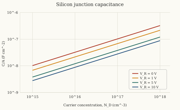
Calculated junction capacitance per area. Each curve has log-log slope \(1/2\).
Thus every curve has slope \(1/2\); reverse bias shifts a curve downward by widening the depletion region.
Problem 4.3: Built-in voltage from Table 4.1
Brief solution
1. Method.
The area is constant, so multiplying \(1/C^2\) by \(A^2\) changes only the vertical scale and not the voltage-axis intercept. A least-squares fit to all 21 tabulated points gives, with \(C\) in pF and applied voltage \(V\) in volts,
2. Key step.
3. Answer.
Show detailed steps
The area is constant, so multiplying \(1/C^2\) by \(A^2\) changes only the vertical scale and not the voltage-axis intercept. A least-squares fit to all 21 tabulated points gives, with \(C\) in pF and applied voltage \(V\) in volts,
Set the fitted ordinate to zero:
Therefore,
Problem 4.4: Area and response time
Brief solution
1. Method.
For a device of thickness \(d\), resistivity \(\rho\), permittivity \(\epsilon\), and area \(A\),
2. Key step.
3. Answer.
which is independent of area.
Show detailed steps
For a device of thickness \(d\), resistivity \(\rho\), permittivity \(\epsilon\), and area \(A\),
Their product is
which is independent of area.
The complete circuit also has an external resistance \(R_L\):
In the usual reverse-biased photodiode, \(R_D\gg R_L\), so
The fixed load breaks the internal area cancellation. A smaller junction has less capacitance and is therefore faster, until transit time or another parasitic becomes the dominant limit.