Chapter 9: Electro-Optic Modulators
Source: Hunsperger, sixth edition (2009), Problems 9.1–9.11, printed pages 195–198. Use \(\delta n=-n^3rE/2\) for the appropriate principal polarization, with sign selected by crystal orientation.
Problem 9.1 — Compensated GaP phase modulator
Working. The carrier difference is \(\Delta N=2.999\times10^{18}\,{\rm cm}^{-3}\). Using the stated \(m^*=0.013m_0\) in the carrier-cutoff relation,
The breakdown field is \(5\times10^7\) V/m, so \(V_{\max}=E_ct=27.48\) V. Convert \(r_{41}=5\times10^{-11}\,{\rm cm/V}\) to \(5\times10^{-13}\,{\rm m/V}\). With \(n=3.2\),
Answer. Limiting thickness 0.5496 micrometres, limiting voltage 27.48 V, and ideal uniform-field pi-shift length 0.769 mm.
Check. Operate slightly above cutoff and below breakdown in practice. The estimates assume full optical overlap with the uniform field; the poorly confined cutoff mode would not actually have unit overlap.
Problem 9.2 — Voltage needed to turn on a GaAs guide
Data. The drawing supplies \(t=3\,\mu{\rm m}\), \(N_2=10^{15}\), \(N_3=3.80\times10^{17}\,{\rm cm}^{-3}\), and \(n_3=3.4\). Use the chapter’s GaAs coefficient \(r_{41}=1.4\times10^{-12}\,{\rm m/V}\).
Working. At 1 micrometre the Drude contrast with mass \(0.08m_0\) is 0.000624917. The asymmetric fundamental requires approximately \(\Delta n_c=1/[32(3.4)(3^2)]=0.00102124\). The electro-optic effect must supply the difference:
Answer. Approximately 43 V is the cutoff estimate; slightly more is needed to produce a bound fundamental.
Check. The existing carrier contrast must be subtracted. This calculation uses the requested uniform voltage-drop approximation.
Problem 9.3 — Schottky modulation and the Franz–Keldysh effect
Working. Reverse bias changes the depletion field, which changes both refractive index and near-edge absorption. Index change directly produces phase modulation; birefringence can alter polarization. Interference or an analyzer converts phase/polarization changes into intensity changes. A time-varying phase produces instantaneous frequency change \(\delta\omega=-d(\delta\phi)/dt\) for the chosen complex-field convention. A binary drive can encode pulses.
Answer. All listed signal formats are possible with appropriate device and readout arrangements; intensity is not automatically produced by a purely phase-modulating element alone.
Check. Franz–Keldysh electroabsorption is field-assisted sub-gap absorption associated with band tilting and tunnelling. It is not a uniform permanent reduction of the material’s zero-field bandgap.
Problem 9.4 — Polarization dependence
Working. The electro-optic response is tensorial: \(\Delta(\epsilon^{-1})_{ij}=r_{ijk}E_k\). The optical polarization samples particular principal-axis changes. Rotating polarization can select different coefficients, reverse the phase response, or select an eigenpolarization with little response.
Answer. Polarization generally strongly affects modulation depth. Crystal cut, electrode direction, and optical polarization must be specified.
Check. An isotropic scalar-index approximation cannot predict polarization switching. Phase depth and detected intensity depth also depend on the analyzer or interferometer.
Problem 9.5 — Two conditions for synchronous transfer
Working. The interacting modes need matching longitudinal phases, \(\beta_0=\beta_1\), so their incremental transfers do not cancel. They also need a nonzero coupling integral, normally supplied by overlapping evanescent tails with compatible field symmetry and polarization.
Answer. Phase matching and spatial/modal overlap.
Check. Sufficient interaction length is then required: \(\kappa L=\pi/2\) for complete first transfer. Identical propagation constants in widely separated guides do not transfer appreciable power.
Problem 9.6 — Directional-coupler switching voltage
Working. With \(\kappa=1\,{\rm cm}^{-1}\), \(L=\pi/(2\kappa)=1.5708\) cm. The first detuned zero needs \(|\Delta\beta|=\sqrt3\pi/L=2\sqrt3\,{\rm cm}^{-1}\). Thus \(|\Delta N|=\sqrt3\lambda_0/\pi=5.844\times10^{-5}\) for wavelength in centimetres.
Using the Table 4.2 index \(n\simeq3.47255\) at 1.06 micrometres, full electro-optic overlap, and electrode separation 5 micrometres,
Answer. (a) 1.5708 cm. (b) Approximately 14 V under the stated uniform-field/material-index assumptions.
Check. Only one channel is tuned. Push–pull tuning of both channels changes the voltage relation, and a nonunit overlap increases the required voltage.
Problem 9.7 — Compare plasma and electro-optic index changes
Working. With the GaP parameters of 9.1, the Drude relation gives \(\Delta n_{\rm carrier}=0.0128326\). Matching that magnitude by a uniform electro-optic field across the limiting thickness requires
Answer. (a) About 0.01283. (b) About 861 V in the ideal uniform-field calculation, already far beyond the 27.48 V breakdown estimate. (c) A uniformly doped Schottky depletion region has a triangular, not nearly uniform, field; the same numerical voltage cannot simply be reused as an exact answer.
Check. At fixed depletion width and fixed peak field, a triangular field drops half the voltage of a uniform field. For the actual guided mode, the relevant change is a field-weighted overlap, so a self-consistent depletion and mode calculation is needed.
Problem 9.8 — Field profiles for compensated and uniform material
Working. Poisson’s equation gives \(dE/dx=eN_D/\epsilon\). A nearly compensated layer has small slope, so its field is almost constant across the layer and then drops rapidly in the heavily doped substrate. A uniformly doped depletion region instead has \(E(x)=eN_D(W-x)/\epsilon\).
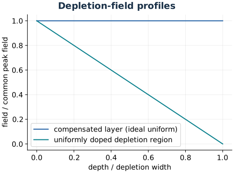
Normalize both examples to the same depletion width; voltage is area under each field curve.
Answer. Draw a nearly flat profile for the compensated guide and a linear triangular profile for uniform doping. Increasing doping increases the field gradient and its influence on the index profile.
Check. Index perturbation follows the tensor-weighted local field, while depletion width itself depends on voltage and doping.
Problem 9.9 — Electrical drive power for a phase swing
Working. Let voltage denote peak sinusoidal amplitude: \(\Delta\Phi=\pi Ln^3rV/(\lambda_0t_g)\). With \(C=\epsilon A/t_g\) and \(R_L^{-1}=2\pi C\Delta f\), the average load power is \(P=V^2/(2R_L)=\pi C\Delta f\,V^2\). Substituting for \(V\) yields
Answer. This is the requested result.
Check. \(A\) must be the electrode-overlap area used by the capacitance model. Using RMS voltage without adjusting the peak phase definition creates a factor-of-two discrepancy.
Problem 9.10 — Bandgap for a near-edge absorption modulator
Working. The 1.15 micrometre photon has energy \(E_\gamma=1.239841984/1.15=1.07812\) eV. Choose a zero-field gap slightly above this energy, leaving low off-state interband absorption while allowing the applied field to increase the absorption tail at that photon energy.
Answer. A material with gap near, and modestly above, 1.08 eV.
Check. A gap far below the photon energy gives excessive off-state absorption; a gap far above it may require an impractically large field.
Problem 9.11 — Insertion loss and extinction
Working. The high-transmission and low-transmission states have \(T_{\rm on}=e^{-0.2(2)}\) and \(T_{\rm off}=e^{-2(2)}\). Therefore
Answer. Insertion loss 1.737 dB; extinction ratio 15.63 dB. For 500 mW incident, outputs are approximately 335.16 and 9.158 mW.
Check. The input power cancels from both decibel ratios. Extinction uses the difference of absorption coefficients.