Chapter 18: Quantum-Well Devices
Source: Hunsperger, sixth edition (2009), Problems 18.1–18.9, printed pages 398–399.
Infinite-well convention
For well width \(L_z\), a subband edge is \(E_n=\hbar^2\pi^2n^2/(2m^*L_z^2)\). Including spin degeneracy, each occupied 2D subband adds \(m^*/(\pi\hbar^2)\) to density of states per area per energy. The number of states integrated up to energy has linear segments; the density of states itself has steps.
Problem 18.1 — MQW versus superlattice
Working. Multiple wells with thick barriers have nearly independent confined states: tunnelling between neighboring wells is weak. With thin barriers, adjacent wavefunctions overlap and the repeated potential forms coupled minibands along the growth direction.
Answer. MQW normally denotes substantially isolated wells; superlattice emphasizes coherent coupling and miniband formation.
Check. Merely counting the number of layers cannot distinguish them. Barrier thickness and electronic coupling are decisive.
Problem 18.2 — GaAs subband steps
Working. State the material assumption \(m_e^*=0.067m_0\). With \(L_z=7\) nm,
The step magnitude is
Answer. Equal DOS jumps occur at those three energies. For the \(100\,\mu{\rm m}\times100\,\mu{\rm m}\) area, each whole-well DOS step is \(2.79880\times10^9\,{\rm eV}^{-1}\).
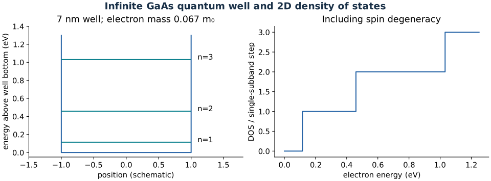
The idealized first three GaAs conduction subbands.
Check. Energies scale as \(n^2\), whereas each DOS step has the same height. The infinite-barrier assumption becomes poor for high subbands above a real barrier.
Problem 18.3 — Fundamental interband quantum-well emission
Working. Electron and hole confinement both increase transition energy. With stated approximations \(E_g=1.43\) eV, \(m_e^*=0.067m_0\), and heavy-hole mass \(m_h^*=0.5m_0\),
Answer. \(\lambda_0=1.239841984/E_\gamma \simeq0.79483\,\mu{\rm m}\).
Check. The hole term adds despite being plotted downward in an electron band diagram. Finite barriers, excitons, and the selected valence band shift the actual wavelength.
Problem 18.4 — SEED optical feedback and logic
Working. Absorbed light changes the current in an MQW p-i-n diode. In an appropriate electrical load circuit, that current changes diode voltage. The quantum-confined Stark effect makes absorption depend on that voltage, closing a feedback loop. Suitable load lines can yield two stable optical/electrical states.
Answer. This self-consistent absorption-voltage feedback enables bistability and therefore potential binary switching or logic.
Check. A bare passive MQW layer is not automatically bistable. The bias circuit, optical operating point, and feedback sign matter.
Problem 18.5 — Six-nanometre well and twenty-well gain
Working. With \(E_g=1.52\) eV and the same GaAs electron/heavy-hole masses as 18.3, the 6 nm infinite well gives \(E_{1e}+E_{1h}\simeq0.17679\) eV. Thus \(\lambda_0\simeq1.239841984/1.69679=0.73070\,\mu{\rm m}\).
For independent equally pumped wells, modal gain sums: \(g_{\rm modal}=\sum_j\Gamma_jg_{{\rm mat},j}\).
Answer. (a) Approximately 730.7 nm within the infinite-well model. (b) If 80 inverse centimetres is each well’s modal contribution and all overlaps remain equal, twenty contribute 1600 inverse centimetres.
Check. If 80 is material gain, it does not automatically multiply by twenty. Optical confinement, carrier distribution, and total layer thickness must be specified. A high infinite-well level may not be bound in a finite AlGaAs barrier.
Problem 18.6 — QCSE extinction for two propagation geometries
Working. The absorption change is \(\Delta\alpha=2000-10=1990\,{\rm cm}^{-1}\). For perpendicular passage through 10 micrometres,
For parallel passage over 50 micrometres with confinement 0.8, the exponent is \(1990(0.8)(0.005)=7.96\).
Answer. Ratios are 7.316 (8.642 dB) and 2864.07 (34.57 dB), respectively.
Check. Compare ratios of transmitted states, not absorbed fractions. The confinement factor multiplies the absorption-length product.
Problem 18.7 — InGaAs subband density of states
Working. Substitute the supplied electron mass \(0.045m_0\) and 7 nm width:
Answer. Equal steps occur at those energies. Multiplying by the stated area gives \(1.87979\times10^9\,{\rm eV}^{-1}\) per whole-well step.
Check. The hole mass does not enter the requested conduction-band DOS. The lighter electron mass raises confinement energy and reduces DOS step height compared with GaAs.
Problem 18.8 — Temperature-dependent threshold
Working. Use the empirical characteristic-temperature law \(I_{\rm th}(T_2)/I_{\rm th}(T_1)=e^{(T_2-T_1)/T_0}\). Temperature differences have the same numerical value in kelvin and degrees Celsius:
Answer. Approximately 10.58 mA.
Check. \(T_0\) is a fitted temperature scale, not a temperature to which 273.15 must be added in this ratio.
Problem 18.9 — Why quantum wells can narrow laser linewidth
Working. A step-like electronic DOS and strong differential gain can reduce the carrier-number change needed to alter stimulated emission. The associated amplitude-phase coupling and spontaneous-emission contribution to the lasing mode can be reduced in a well-designed QW laser.
Answer. Quantum confinement can improve differential gain and noise/phase dynamics, producing a narrower line at comparable operating conditions.
Check. Linewidth also depends on cavity loss, output power, linewidth-enhancement factor, temperature, and technical noise. Adding wells alone does not guarantee a narrower spectrum.