Chapter 14: Heterostructure, Confined-Field Lasers
Source: Hunsperger, sixth edition (2009), Problems 14.1–14.10, printed pages 298–299.
Problem 14.1 — One possible 850-nanometre DH laser
Working. The desired photon energy is \(1.239841984/0.85=1.45864\) eV. Using the approximate 300 K direct-gap relation \(E_g(x)\simeq1.424+1.247x\) eV gives active composition \(x\simeq0.028\). Choose Al0.3Ga0.7As confining layers. Table 4.2 then gives approximate optical indices \(n_a=3.59486,\ n_c=3.40316\).
For a symmetric core, the first excited TE/TM cutoff is \(d_c=\lambda_0/[2\sqrt{n_a^2-n_c^2}]=0.36693\,\mu{\rm m}\). Choose a 0.15 micrometre active layer between thick n-type and p-type claddings, with doped contact caps outside the optical tails.
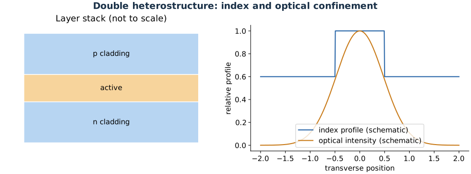
A symmetric optical DH design; doping supplies carrier injection.
Answer. This illustrative design supports TE0 and TM0 only; take claddings thick enough to isolate the contact regions, for example 1.5 micrometres after checking tail decay.
Check. The mode roots are approximately 3.45625 and 3.45010. This is not a unique design, and band filling, temperature, and composition calibration shift the exact emission wavelength.
Problem 14.2 — Homojunction, single-, and double-heterostructure lasers
Working. A homojunction lacks heterobarriers, so carriers and light spread beyond the active region. A single heterojunction confines one side, reducing leakage and improving overlap asymmetrically. A double heterojunction places the active material between higher-gap, lower-index layers, confining both carrier types and the optical mode.
Answer. DH structures generally lower threshold and improve efficiency, at the cost of more demanding epitaxial growth and interface control. SH provides an intermediate compromise.
Check. Carrier confinement comes from band offsets; optical confinement comes from refractive-index differences. Both mechanisms are needed to explain the improvement.
Problem 14.3 — Unequal-mirror threshold density
Working. A round trip multiplies intensity by \(R_1R_2e^{2(\Gamma g-\alpha)L}\). At threshold this is one, giving \(\Gamma g_{\rm th}=\alpha+(2L)^{-1}\ln[1/(R_1R_2)]\). Substitute the book’s current-gain relation \(g=\eta_q\lambda_0^2J/(8\pi en^2d\Delta\nu)\) and \(\Gamma=d/D\).
Answer. The active thickness cancels within the \(d/D\) model; the modal thickness \(D\) remains.
Check. Equal mirrors reduce to \(L^{-1}\ln(1/R)\). A perfectly reflecting end leaves only half the other mirror’s logarithm.
Problem 14.4 — Thin-layer confinement as a function of composition
Working. Set \(n_c(x)=3.590-0.710x+0.091x^2\) and \(n_a=3.590\). The thin-layer estimate is
For \(d=0.1\,\mu{\rm m},x=0.1,\lambda_0=0.9\,\mu{\rm m}\), \(\gamma=1.21441\,\mu{\rm m}^{-1}\) and \(\Gamma\simeq0.12144\).
Answer. About 12 percent confinement, consistent in scale with the small-thickness portion of Fig. 14.4. Retaining the exponential integral gives \(1-e^{-\gamma d}=0.11436\) within that model.
Check. Although written \(\gamma d\), the estimate scales as \(d^2\) because \(\gamma\) itself depends on thickness. It must not be extrapolated above unity.
Problem 14.5 — Forward-biased band diagram and carrier barriers
Working. Draw a conduction-band well and a valence-band well in the lower-gap active layer. Forward bias reduces the junction barrier and separates electron/hole quasi-Fermi levels. The conduction-band steps hinder electrons leaving the active region; valence-band steps hinder holes leaving it.
Answer. Label both band offsets and the injected carrier populations; above threshold their separation supports a gain window.
Check. The optical field confinement shown in the DH figure is not itself a carrier potential. Carrier barriers are energies, not refractive-index steps drawn on the same numerical axis.
Problem 14.6 — Why use a stripe geometry?
Working. Restricting current injection to a narrow stripe reduces the electrically pumped area and therefore threshold current. Lateral gain or index guiding improves overlap and can limit transverse mode count. The narrower emitting region also improves coupling to a small optical mode.
Answer. Lower total threshold current, improved lateral mode control, and more useful output geometry than broad-area pumping.
Check. Stripe width does not automatically set longitudinal single-mode behavior. Very broad stripes can show filamentation and spatial hole burning; very narrow stripes can increase resistance.
Problem 14.7 — Quantum-to-power efficiency conversion
Working. The photon energy at 0.9 micrometres is 1.37760 eV. An incremental injected electron supplies 2.5 eV electrically, so
Answer. 16.53 percent differential power efficiency.
Check. As in 12.10, total wall-plug efficiency depends on operating current and threshold overhead. The supplied differential efficiency does not determine it exactly.
Problem 14.8 — Antireflection coating at the gain limit
Working. For \(\Gamma=1\), modal gain available above internal loss is \(70-5=65\,{\rm cm}^{-1}\). Equal mirrors satisfy \(\ln(1/R)/L=65\) at threshold.
Answer. About 14.23 percent intensity reflectivity at each end.
Check. This repeats the physical parameter set of 12.11. Changing both mirrors rather than one is essential to that result.
Problem 14.9 — Explain the DH improvements
Working. Larger-gap surrounding layers suppress electron and hole leakage, improving injection efficiency. Their lower optical index keeps more field in the gain region, raising \(\Gamma\). Both changes reduce required current, heating, and unwanted absorption outside the active layer.
Answer. Lower threshold, greater useful differential efficiency, and improved prospects for continuous room-temperature operation follow from simultaneous electrical and optical confinement.
Check. Benefits are not merely the presence of extra interfaces. Poor interfaces introduce defects and recombination and can erase them.
Problem 14.10 — Why the heterostructure advance mattered
Working. Early semiconductor lasers needed high current densities and stringent cooling. Heterostructures concentrated both carriers and photons, making efficient compact sources practical for optical communication. The same bandgap-engineering idea supports many other high-performance semiconductor devices.
Answer. The 2000 Physics Nobel recognition of Zhores Alferov and Herbert Kroemer reflected the importance of semiconductor heterostructures to high-speed electronics and optoelectronics.
Check. The historical recognition concerns the broad enabling heterostructure technology; attributing it solely to a particular modern laser package would be too narrow.